Rutherford Appleton Laboratory (RAL) is located on Harwell Campus, situated near the village of Harwell in south Oxfordshire. This multidisciplinary laboratory has over 60 years of history of scientific research and engineering.
The Particle Physics Department at RAL is involved in the construction and upgrades of many experiments across all areas of high energy physics. Many of our facilities are suitable for academic and industrial use outside particle phyics.
All contact information has been obtained with permission. Available equipment is subject to change and is not guaranteed.
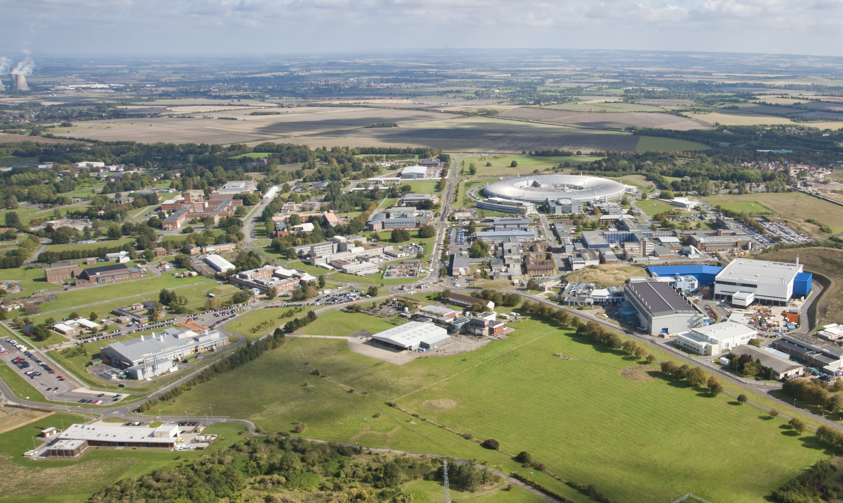
Aerial View of Harwell Campus including RAL
Irradiation
X ray radiation facility
This facility is well-suited to users seeking to
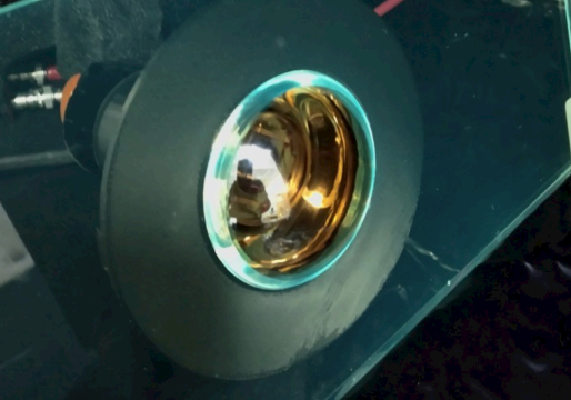
Interior of PPD's Seifert RP149 model X ray irradiation machine
Contact: craig.sawyer@stfc.ac.uk
- PPD possesses beta sources of radiation, currently being used for the testing of sensors.
Cryogenics and temperature control
- PPD has a dry cabinet and freezer for storage of semiconductor devices. Capable of maintaining temperatures of –40C.
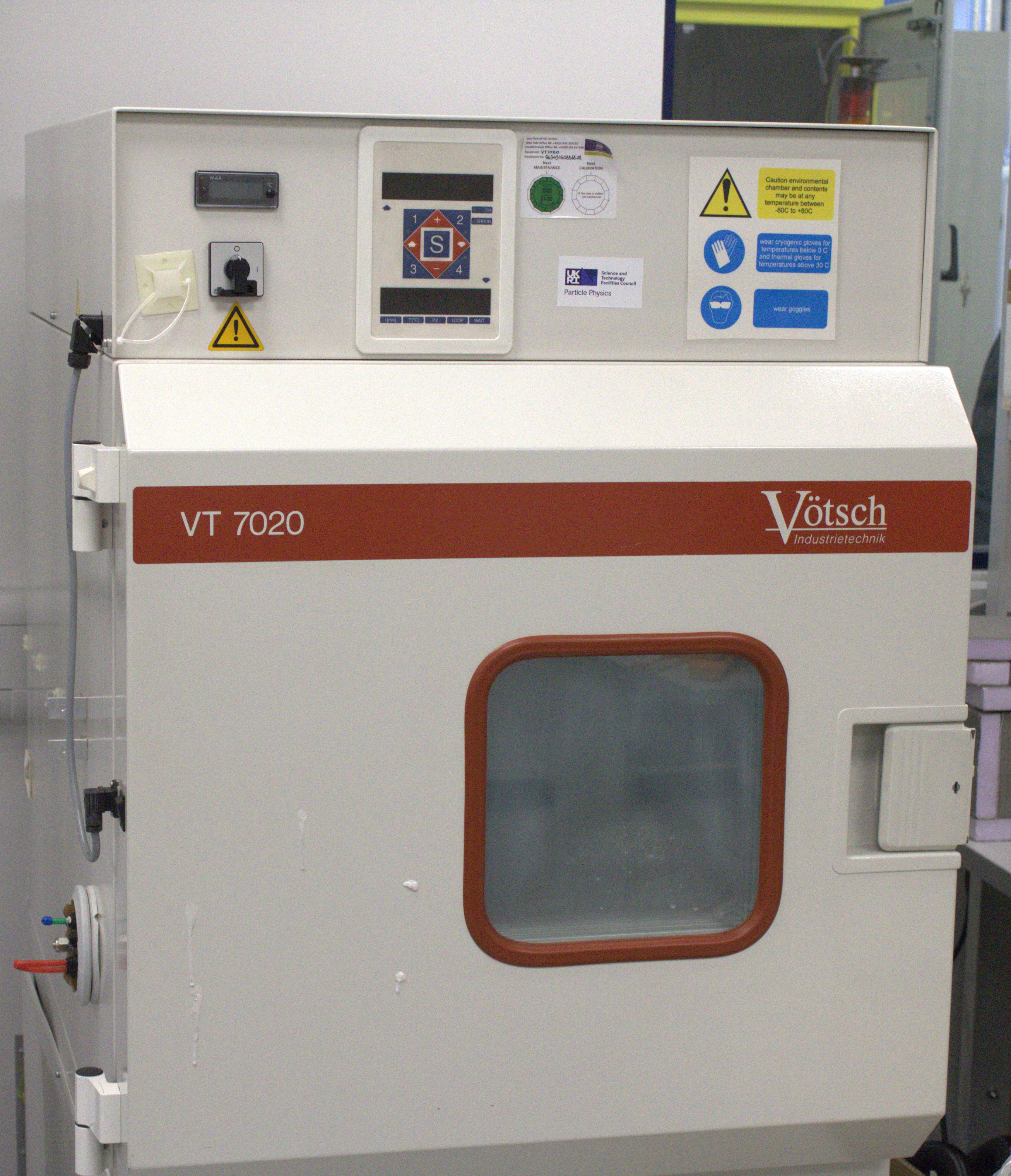
V7020 model climate chamber developed by Vötsch Industrietechnik. The V7020 model provides a spacious 110L of volume.
This particular model can produce static or dynamic temperature environments of -70 to +70°C
This model is capable of thermal cycling at a rate of 10°C / min.
This versatile climate chamber can offer rapid temperature flucuations and a generous amount of room, allowing for a variety of applications.
Contact: ben.smart@stfc.ac.uk
Cold Radon Emanation Facility
CREF is unique among other high sensitivity radon emanation facilities, with a low temperature capability. This allows the measurement of emanation via radon recoil from surfaces and radon diffusion as a function of temperature.
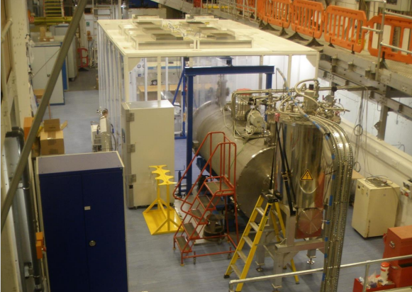

Cold Radon Emanation Facility: Shortly after its commissioning in 2022 (Left) CREF logo (Right)
- Assays can be conducted from room temperature to 80K, generating valuable data of radon outgassing.
- The facility consists of an ISO 7 class clean room containing the radon concentration line, radon detector and a workstation for experimental analysis. A layered 500L cryogenic vacuum chamber through which purified nitrogen gas circulates, this provides constant thermal contact with the 200L test chamber it encompasses.
- 200L test chamber allows for the radiopurity of large material samples to be assessed.
- CREF was only recently commissioned, with calibration and specification charaterisation completed in 2023. Throughout 2024, there have been developments of its DAQ system, with installation expected shortly.
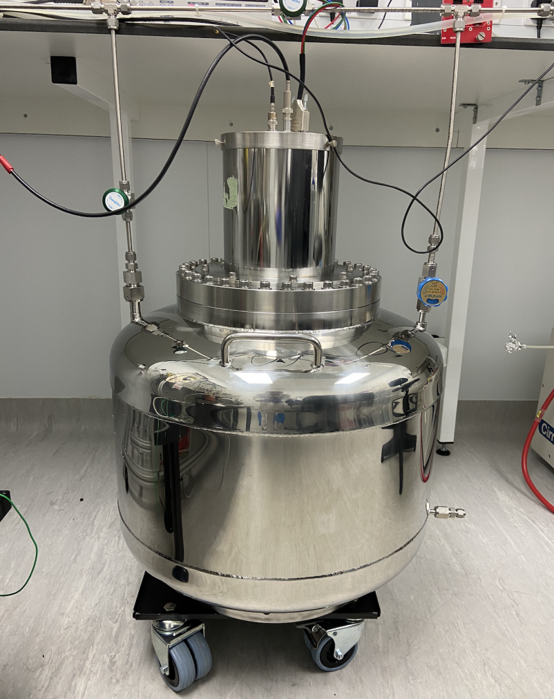

Cold Radon Emanation Facility 80L Electrostatic detector vessel (Left). 200L Emanation chamber with 800L cryogenic vessel capable of cooling down to 77k.
This unique facility has a wide range of applications
- CREF is expected to play a major role in determining radiopurity requirements for the components of the next generation of dark matter detector, XLZD. Ideal for Industry/ academic institutions engaged in the manufacture of XLZD or related dark matter components.
- CREF also has the potential to explore novel methods of radon emanation suppression techniques such as chemical treatments or physical barriers.
Contact: mark.tucker@stfc.ac.uk
WLCG Tier-2 computing centre
Alongside the the UK Tier-1 centre managed alongside SCD, PPD manages a combined Tier 2/3 facility. It maintains data from ATLAS, CMS and LHCb experiments as well as handling job submission from over 20 virtual organisations.
- PPD is responsible for the High Throughput main batch system of approximately 8000 CPU cores with over 8PB of disk data storage. Job availability and further technical specifications are provided here RAL Tier-2
- Our tier 2 facility also has 20 high end GPU cards of varying models, with potential for machine learning development.
- 2 FPGA developmental boards designed for machine learning applications.
PPD has a dedicated laboratory for the testing and debugging firmware for FPGA boards and possibly GPU boards, with a subsidiary role in electronic communications.
- Workstations are connected to both a Particle Physics Department network and a hardware network.
- This flexible network configuration allows for dedicated data analysis.
- Within PPD these workstations have been used for data acquisition system development and real time processing.
- Rack based electronics tests FPGA boards from a variety of experiments.
The laboratory is not dedicated to one single experiment, previously testing DUNE FPGA boards and currently assessing FPGA boards intended for the CMS and ATLAS HL-LHC upgrade.
As of writing (November 2024), the laboratory testing racks have unoccupied racks primed for testing.
Contact: kristian.harder@stfc.ac.uk
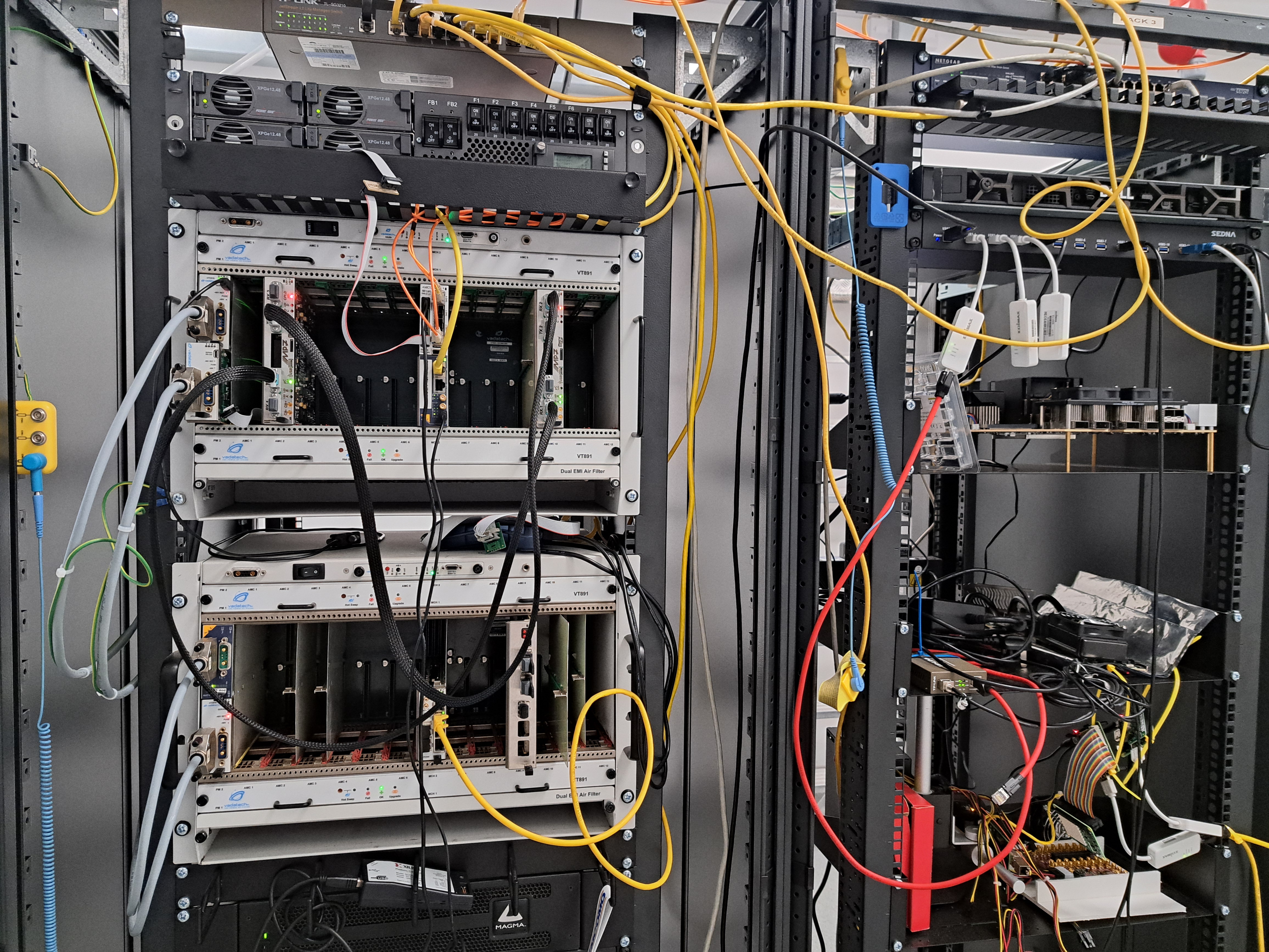 Circuit boards intended for the ATLAS experiment being tested.
Technology Computer Aided Design (TCAD) is a software tool licensed via Synopsys. TCAD runs sophisticated simulations that provide detailed characterisations of semiconductor devices.
- RAL can provide multiple workstations with TCAD software allowing for data intensive jobs to be conducted simultaneously.
- PPD has used TCAD to both optimise and design semiconductor detectors/ sensors for various components of the ATLAS semiconductor tracker.
Oscilloscopes
PPD possesses two powerful oscilloscopes that occupy a wide range of frequencies.
- Depicted below is Digital oscilloscope that that can generate 8-bit signals through 4 signal channels with a frequency of up to 33GHz. This model is an optical signals probe.
- PPD also makes use of a mixed signal oscilloscope. This generates electronic signals with a lower frequency range of up to 4GHz.
RAL has a 600m2 Cleanroom which is managed by the TD. This highly controlled environment is split into 2 sections. 440m2 ISO 7 class section is dedicated to detector systems. For instance, they were used and are currently engaged in manufacture / assembly of ATLAS ITk pixel end caps and strip staves.
160m2 is dedicated to an ISO 5 class section, used for semiconductor device assembly and testing.
Please bear in mind this is not a complete list of equipment within the Cleanroom. For the sake of brevity, it has been reduced to include some of the equipment and their applications.
- Fine wedge bonding: Hesse and Knipps manufactured wedge – wedge bonder. 2 BJ820 and BJ855 models are available. Capable of micrometer precision to 20µm and 25µm. The latter models are capable of reconfiguration for Au-ball and Au-Stud bonding.
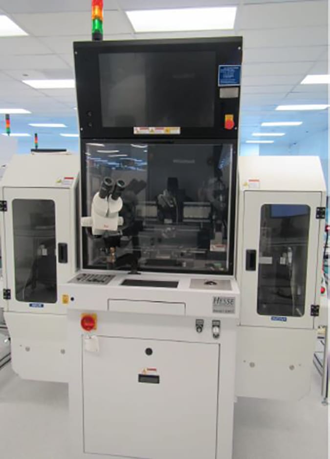
 BJ855 model (Left). Technology staff members testing readout chips for Darkside-20K Silicon Photomulitpliers in the R115 (right).
- Flip Chip bonding: Setna produced chip bonder models FC150 and FC300. Allowing for chip placement up to 1.5µm and 0.5µm accuracy respectively.
- Optical Profilometry: Cyber Technologies CT100 model is a high powered, non-surface contact, capable of distinguishing features by 3nm across 150mm2 scanning area.
- Mounting / Testing Wafers: Cascade manufactured automatic and manual probe stations for mounting and testing assembled wafers.
- High magnification microscopes: Keyence and Leica manufactured digital microscopes. These both feature ultra-high magnification, with the latter offering image and video recording capabilities as well as HDR imaging and stitching functions.
For a complete list of the equipment and commercial availiability please contact : John.Lipp@STFC.ac.uk
Semiconductor characterisation
We have equipment that conducts precise device measurements and tests electronic circuity. PPD has made use of this for wafer fabrication for the ITk staves for the ATLAS experiment.
Within the ISO 5 Class clean room, there are two sets of specialised probe stations. This equipment is able to characterise semiconductor devices or chips and perform precise device measurements.
- 2 models in our possession (both depicted below) are capable of loading 8 inch or 12-inch silicon wafers onto them respectively.
- The former possesses complex hardware which characterises semiconductor devices to high resolution. A 100x microscope is used to position manipulators to micrometer precision.
- The latter is primarily used within wafer fabrication. Automatically mounting chips onto the silicon wafer in a stepwise fashion until the assigned task is complete.
- This model possesses custom electronics on the probe station, allowing for preliminary testing of the chip performance once mounted.
- Further testing and inspection then are conducted by an in-house workstation which maps each chip, measuring various parameters associated with performance for each.
On the left is the 8-inch model, primarily used for semiconductor characterisation. On the right is the black 12-inch model, primarily used for wafer fabrication.
- In addition to these probe stations, laboratory 5 possesses dry storage for electrical devices as well as several data acquisition testing workstations.
- These probe stations can provide detailed assessments of chip performance, helping to inform on modifications or prompt input parameter changes.
Laser charge injection systems
- Below depicts one of two laser injection systems. This produces a laser operating at wavelengths within a UV to infrared range. Pulse rate can deliver beams to micrometer precision at a MHz frequency.
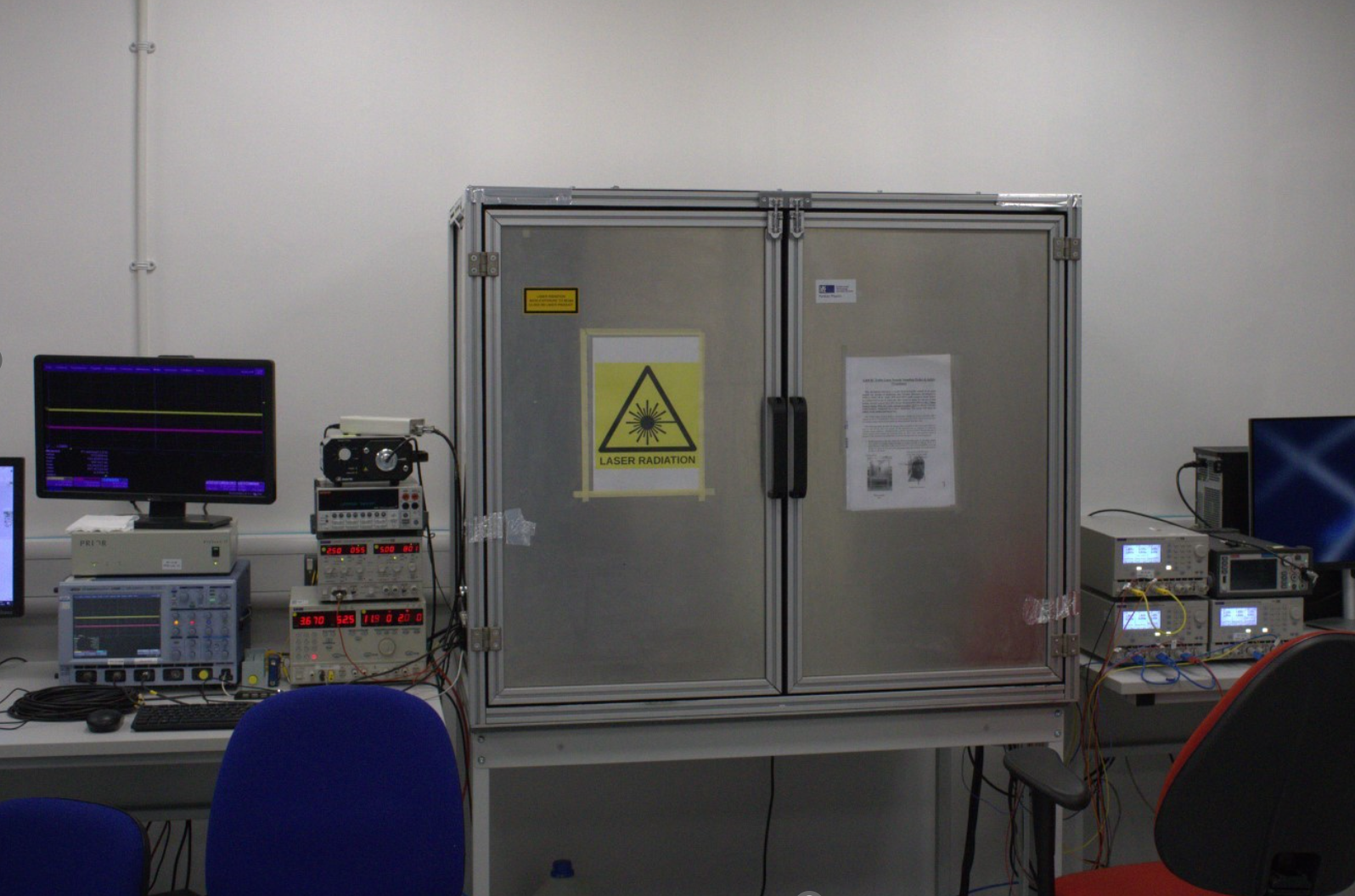
Below image is an UCT model. Shares similar micron precision as above although only operates within UV wavelengths and has a higher pulse rate on the order of picoseconds.
At PPD these laser charge injection systems are used to conduct a variety of sensor testing for a wide range of experiments. Many applications exist for industrial, nuclear or particle physics sensor components.
Contact: atanu.modak@stfc.ac.uk
Experiment specific facilities
HyperK test frame is a 4.2m x 2.8m steel frame, consisting of 6 x 4 of 0.7m2 grids. Its design has been adapted to mimic the entire HyperK frame within the cavern, scaled down by a factor of 15.
HyperK test stand is available to HyperK collaborators developing various components. Users can practice component assembly, for the determination of the most efficient assembly order, estimate assembly timing and review component design.
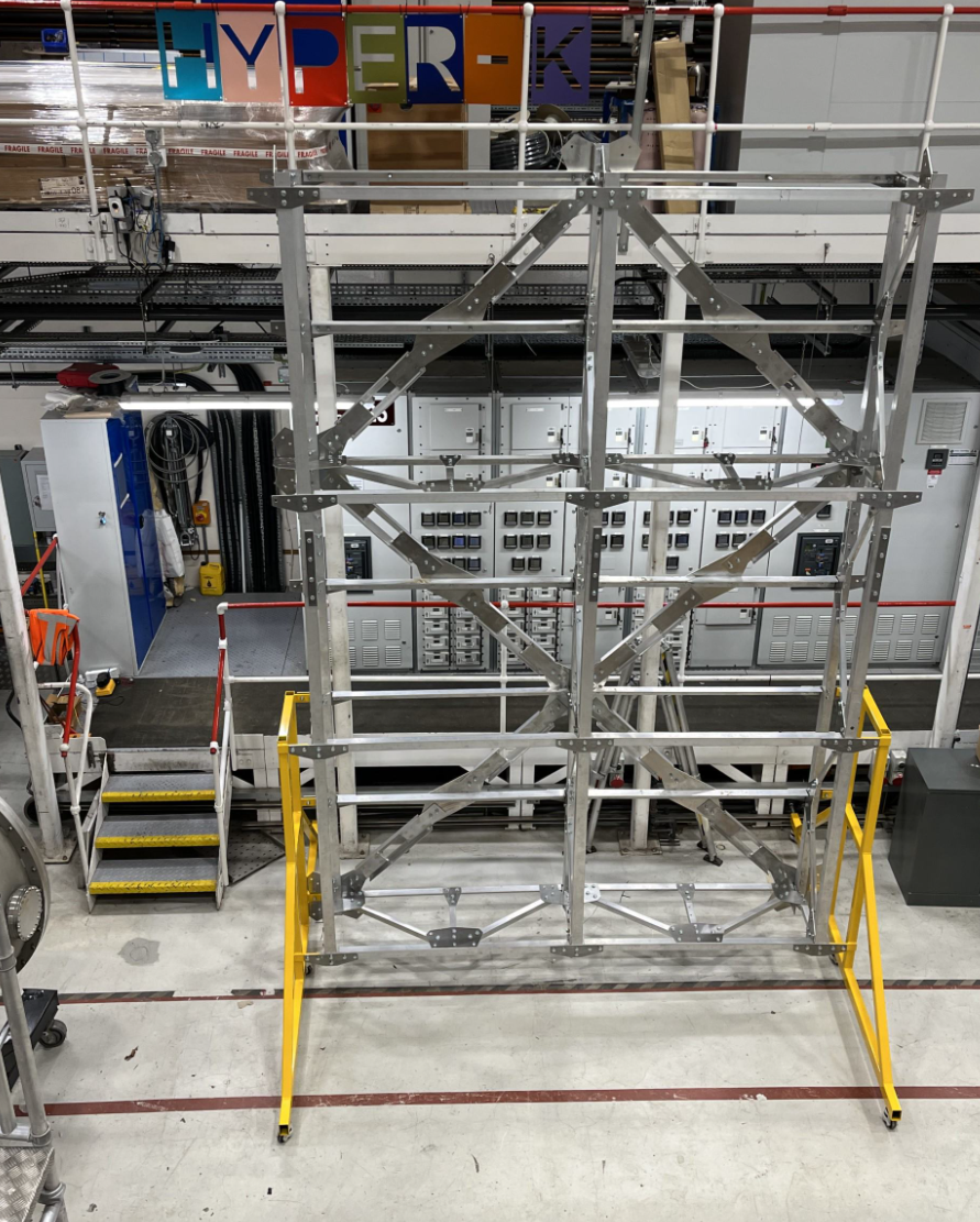
Hyper-K test stand following its assembly. Photo taken in 2023.
For HyperK collaborators looking to use the mock frame
Unavailiable facilities
The following facilities are cccupied with ongoing research and not available as of writing (November 2024)
PPD is engaged with the testing of outer detector photomultipliers.
Example of Photodiode and WLS plate tested in PPD Lab 7
- This laboratory is dedicated to the performance of outer detector photomultipliers provided by the Hyper-K collaboration.
- Separated from the inner detector by a light occluding layer, the outer detector photomultiplier’s purpose is to exclude cosmic ray muon events from neutrino interactions.
- PPD is currently evaluating different models to determine those with the greatest sensitivity and set limits for signals that produce overwhelming currents.
No contact: Facility is unavailable to external users
- Purpose built cryostat specifically for testing of printed circuit boards (PCBs) with silicon photomultipliers (SiPM).
- Liquid nitrogen cools 2 nested boxes of installed SiPMs to lower their count rate allowing for assessment of their radiation hardness
PPD is using this cryostat in the research and development of SiPM that may be used within the LHCb. PPD is part of an international collaboration assessing SiPMs for their potential application within this upgrade.

LHCb SiPM PCB cryostat
No contact: Facility is unavailable to external users
